I am Article Layout

Select your investor profile:

This content is only for the selected type of investor.

Semiconductor industry's impact on environment

December 2023
Marketing Material

Are semiconductor companies a growing environmental problem or a green solution?

The semiconductor industry's environmental credentials are under intense scrutiny. But chips are also essential to the net zero transition.

A view that is gaining wider currency among environmentalists is that the semiconductor industry is damaging the planet. It is a justified concern. Chips are manufactured in huge, resource-hungry fabs, factories that can span up to 1 million square feet in size. And each year, the industry uses well over 100 billion litres of water1 and generates nearly 100 million tonnes of greenhouse gas emissions2; it is also a voracious consumer of rare earth metals and produces a lot of toxic waste.

Concerns about semiconductors’ ecological footprint have also been intensifying in recent years as computing has become more powerful and the industry's energy consumption has risen exponentially.  What is more, governments in the US and Europe are about to spend tens of billions of dollars to build domestic chip production capacity. The aim is to ensure reliable supply but it is also certain bring the issues of plant emissions and waste – a once peripheral concern – into sharper relief.

On the face of it, therefore, semiconductors have no place in an environmentally focused portfolio. But on closer inspection, an altogether different picture emerges. 

Powering the green transition with semiconductors

As long-term, responsible investors, we place great emphasis on the environmental credentials of industries and companies when building portfolios. But this also needs to be measured against the crucial role that semiconductors play in the green transition. In other words, it is essential for climate-oriented investors to look beyond the industry's carbon footprint and assess what experts call the ‘handprint’, or the positive impact that it has on the rest of the economy.

For semiconductors, that positive impact is particularly large when it comes to electrification – a key element of decarbonisation.

If we want to reach net zero by 2050, the International Energy Agency estimates that the proportion of electricity within total energy use will have to increase to 50 per cent from the current 20 per cent, replacing fossil fuels.3

That also means that the share of renewable electricity has to rise to 90 per cent from 30 per cent. We need to electrify first, in order to be able to decarbonise. And we also need to cut total energy consumption, which will require a 3 per cent annual improvement in energy intensity of the economy, double the current rate.4  

We believe semiconductors are critical enablers of the green transition.

None of this can happen without semiconductors.

One category of specialised chip, “power semiconductors”, is crucial to facilitating electrification. These chips are used mainly to control the supply of electric power, as well as its conversion (from direct current to alternating current and vice versa), transfer and storage.

Although they represent only around 5 per cent of the overall semiconductor market, or USD40 billion, they have a crucial role to play.5 

In solar power plants, for example, efficient and reliable power semiconductors are required to convert electricity from direct current to alternating current and transmit the power with minimal losses.

Semiconductors are also essential in the modernisation of electricity grids, enabling them to become more responsive to shifts in power supply and demand.

Chips are just as vital for the auto industry. The semiconductor content required for cars is now several times greater than a decade or two ago due to the switch to electric vehicles and the development of smart cars.   

Semiconductors are therefore crucial across the whole electrification value chain, from the development of renewables to grid storage to electric cars and their chargers.

This leaves investors with a conundrum to resolve. How to reconcile semiconductor companies' impact on the natural world with the positive systemic impact of their products?

Planetary Boundaries and Life Cycle Assessment

As managers of the Pictet Global Environmental Opportunities strategy, we approach this problem by using two analytical frameworks which, together, help us gauge a company's contribution to the green transition.

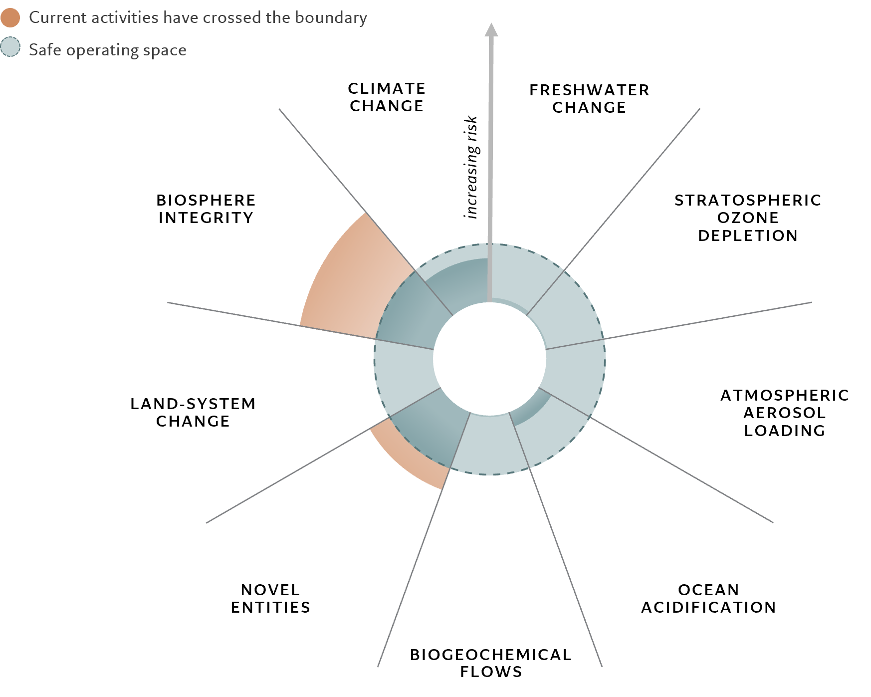
The first is the Planetary Boundaries (PB) model, a science-based framework developed by academics at the University of Stockholm. It analyses the nine environmental dimensions critical to planetary health (including climate change, biodiversity, water and chemical pollution) and, just as importantly, demarcates the “safe operating space” within which human activities should take place.

We apply the PB framework to an investment setting by fusing it into a second framework – Life Cycle Assessment. This tool essentially quantifies the amounts of raw materials, energy, water and the associated emissions that are used or generated throughout a product life cycle. By applying life cycle assessments, we can map the environmental impact of a company along the nine PB dimensions.

Semiconductors' footprint

In Fig. 1, we illustrate how these frameworks are used in practice. Here, the PB-LCA tool is used to quantify the impact a semiconductor equipment manufacturer has on each of the nine planetary boundaries. The analysis shows that this company has a large negative impact on biodiversity, and is also responsible for high levels of chemical pollution (due to hazardous waste and contaminated water, which can be managed through on-site treatment measures). Its environmental impact outside those two boundaries is otherwise negligible. 

Fig. 1 - Measuring up
The footprint of a semiconductor equipment manufacturer across Planetary Boundaries
planetary boundaries
Source: Pictet Asset Management, August 2023. For illustrative purposes only.

Another conclusion to draw from this analysis is that although semiconductors clearly have a significant impact on the environment, it is lower than that of many others. And while the sector’s emissions sound high in absolute terms, they account for only 0.2 per cent of total global emissions.6

Also encouraging is that many companies are working hard to improve their green credentials. Most firms have set targets such as 100 per cent renewable energy and net zero or carbon neutrality over coming years, and the Semiconductor Climate Consortium (SCC) is working towards net zero for the industry as a whole by 2050.7

One way to reduce the footprint is to use extreme ultraviolet (UEV) lithography. It’s a more sophisticated process for transferring patterns onto the silicon wafer surface, which means fewer patterning steps are needed than with traditional UV; this in turn leads to a reduction in emissions.8

Another solution lies in improving abatement, or better treatment of the hazardous and greenhouse gases produced during the manufacturing process. Semi manufacturers are also looking to reduce waste by introducing recycling directly at the fabs.

The green handprint

It is also the case that focusing exclusively on the operations of chip companies does not give a true picture of the industry's environmental credentials. By looking beyond the industry's operations and taking into account the positive contribution semiconductors make to the building of a sustainable economy, investors will be able to draw entirely different conclusions.  

This is where the concept of an industry's “handprint” comes in.

The handprint of a company is the positive effect its products can have on the environmental footprint of its clients. A company creates a handprint when it offers its customers a solution that has a lower footprint than ‘business-as-usual’. Industry practitioners currently apply this concept to carbon emissions but we believe it can be applied more broadly to many other environmental dimensions, including water consumption and use of materials.

The term handprint therefore represents a positive environmental impact and the bigger it is, the better; in theory, the are no limits to it. 

A handprint is difficult to quantify accurately, because it is the difference between a baseline and a counterfactual scenario. So this concept will never realistically be included in climate disclosure rules.

However, we’ve made handprint assessments an important part of our global environmental strategy’s investment process. We want to identify and own those companies that not only minimise their own environmental footprints, but also provide solutions that increase the handprint of their customers and of the rest of the economy. Such companies make up the universe of our investment opportunities.

Our analysis shows that the footprint of a semiconductor equipment manufacturer is dwarfed by their potential handprint. From producing renewable electricity to improving our efficiency in using it, semiconductors have a key role to play in driving the green transition.

Around half of semiconductor and equipment companies generate revenue from products and services that directly contribute to the green transition, such as solar power generation and electric vehicles, according to analysis by MSCI.9 Many others could be involved indirectly.

The impact is hard to quantify, and there are only a handful of studies that are available so we should consider any numbers as rough estimates.  But an analysis by Accenture and the Global Enabling Sustainability Initiative (GeSI) suggested that Information and Communications Technology (ICT) solutions could reduce global emissions by 12Gt CO2 by 2030  (or around a third of what is currently emitted from industry and fossil fuels) and promote sustainable economic growth across mobility, manufacturing, agriculture, buildings and energy sectors.10

To give just a few examples, in the energy sector emissions could be reduced via the deployment of energy management systems, the increase and integration of renewable energy to the grid and the improvement of the efficiency of the grid. And the buildings industry's emissions could be cut by 30-40 per cent through the deployment of Building Management Systems (BMS), which use computers to monitor and adjust a building’s mechanical and electrical equipment such as heating, ventilation, lighting.

None of those savings would be possible without semiconductors – or, indeed, without the tech sector as a whole. The aggregate abatement potential across energy, building and manufacturing adds up to 5.8Gt, almost five times greater than the total footprint of the tech industry.11 And the saving will be much greater if you include other areas, such as agriculture. 

Viewed from this vantage point, semiconductors are key part of the green transition – essential for electrification, which in turn is necessary for decarbonisation.